
Avicena, a privately held company headquartered in Sunnyvale, CA, with a development centre in Edinburgh, recently demonstrated the world’s smallest 1Tbps optical transceiver as part of its LightBundleTM multi-Tbps chip-to-chip interconnect technology. Avicena’s microLED-based LightBundle architecture supports unprecedented throughput, shoreline density and low power, unlocking the performance of processors, memory, and sensors.
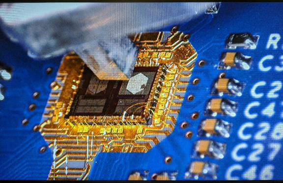
LightBundle 3mm x 4mm ASIC on test board showing LED array and metal ferrule
Artificial intelligence (AI) is driving an unprecedented surge in demand for compute and memory performance, driven by applications like ChatGPT based on large language models (LLMs). These sophisticated models have an insatiable appetite for computing power and fast access to large amounts of memory, resulting in an urgent and growing demand for much higher density low-power interconnects between Graphics Processing Units (GPUs) and high-bandwidth memory (HBM) modules. Today, HBM modules must be co-packaged with GPUs because the GPU-memory electrical interconnect is limited to just a few millimeters in length. Subsequent HBM generations will require IC shoreline densities in the range of 10Tbps/mm or more. Conventional optical interconnects based on VCSELs or Silicon Photonics (SiPh) promise to extend the interconnect reach but struggle to meet size, bandwidth density, power, latency, operating temperature, and cost requirements. By contrast, Avicena’s microLED-based LightBundle interconnects provide higher bandwidth density, much smaller size, much lower power and latency, and very low costs.
“At Avicena we are excited to showcase the world’s most compact 1Tbps transceiver in the shape of a 3mm x 4mm CMOS ASIC using our patented microLED optical interface,” says Bardia Pezeshki, Founder and CEO of Avicena. “Everyone is talking about SiPh solutions for applications in AI clusters. However, for short reach interconnects with less than 10m reach, we believe that our LED based solution is inherently better suited because the compact size, higher bandwidth density, lower power and latency, and temperature tolerance up to 150°C.”
Avicena’s innovations are supported by key investors including Samsung Catalyst Fund, Cerberus Capital Management, Clear Ventures, and Micron Ventures (see press release from August 2nd, 2022, for more details).
“Optical interconnect technology has the potential to improve chip-to-chip and inter-rack performance,” says Marco Chisari, head of the Samsung Semiconductor Innovation Center. “With a roadmap to multi-Tbps capacity and sub-pJ/bit power efficiency, Avicena’s innovative LightBundle interconnects can enable the next era of AI innovation, paving the way for even more capable models and a wide range of AI applications that will shape the future.”
About the Technology
Today’s high-performance ICs use SerDes-based electrical interfaces to achieve adequate off-chip density. However, the power consumption and bandwidth density of these electrical links degrade quickly with length. Conventional optical communications technologies developed for networking applications have been impractical for inter-processor and processor-memory interconnects due to their size, low bandwidth density, high power consumption, and high cost. The typical need for external laser sources (ELS) with SiPh increases complexity and cost.
By contrast the LightBundleTM interconnect architecture is based on arrays of innovative GaN microLEDs that leverage the microLED display ecosystem and can be integrated directly onto compact high-performance CMOS ICs. This enables dense, low-power I/O over the entire area of the IC, resulting in unprecedented shoreline densities. Each microLED array is connected via a multi-core fiber cable to a matching array of CMOS-compatible PDs and the complete LightBundle IC consists of an optical I/O chiplet that is 3D stacked onto an advanced CMOS IC, providing massive data throughput and density at very low energy levels.
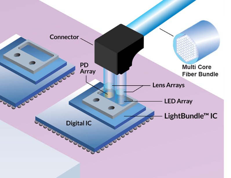
LightBundle optical chiplet construction
“We have previously demonstrated microLEDs transmitting at > 10Gbps per lane and a test ASIC in a 130nm CMOS process running 32 lanes at less than 1pJ/bit.” says Rob Kalman, co-founder and CTO of Avicena, “Now we are bringing up our first ASIC with over 300 lanes and an aggregate bandwidth of over 1Tbps bi-directional at 4Gbps per lane. The ASIC measures less than 12mm2 and contains a full transceiver including the circuitry for the optical Tx and Rx arrays, as well as a high-speed parallel electrical interface and various DFT/DFM functions like BERT, loopbacks, and Open Eye Monitoring (OEM). All key ASIC functionality has been verified and we are currently working on yield improvements for manufacturing scalability.”
The modular LightBundle platform scales to interconnects with tens of Tbps with a shoreline density > 10Tbps/mm. LightBundle is not tied to any foundry process, allowing it to be integrated onto a wide variety of IC process nodes. The compact size, high density, low power, and low latency of LightBundle is ideal for high-density chiplet interfaces like UCIe, OpenHBI, and BoW, and can also greatly extend the reach of existing compute interconnects like PCIe/CXL, and HBM/DDR/GDDR memory links.
About Avicena
Avicena Tech Corp. is a privately held company located in Sunnyvale, CA, with a development centre in Edinburgh, Scotland, is developing LightBundle, a next generation optical interconnect architecture for AI/ML, HPC, sensors, 5G wireless and aerospace applications. This technology revolutionizes High-Performance and Cloud (HPC) computing, which forms the critical hardware on which the Large Language Models (LLMs) of Artificial Intelligence (AI) are running. GaN LED-based interconnects are also capable of operating in extreme environments, which makes them well-suited for other applications, like camera sensors, autonomous vehicles, and aerospace. The company was founded in 2019 by leading technologists from the optical networking industry with a track record of delivering breakthrough products. Avicena’s technology is a key building block in the evolution of networking and computing that will reduce the energy impact on our planet.
For more information, visit https://avicena.tech